Skip to content
What is Thick Film PCB
Thick film PCB is a technology that prints thick layers of conductive and resistive materials onto ceramic substrates, offering high-temperature stability, design flexibility, and durability. It is extensively used in automotive sensors, industrial controls, and aerospace electronics.
1) Origin of Thick Film Circuits
1.1 Reasons for Developing Thick Film Circuits
In the mid-20th century, the electronics industry began exploring new circuit integration methods to meet demands for high reliability under harsh conditions. This led to the emergence of thick film circuits, a technology positioned between traditional printed circuit boards and monolithic integrated circuits. Thick film circuits can remain stable in extreme environments such as high temperature and humidity, thanks to the heat-resistant ceramic substrate and stable thick-film materials. Compared to standard FR-4 PCBs, thick film circuits perform reliably over a wide temperature range (approximately -55°C to +125°C), and are less prone to failure under rapid temperature changes. In addition, thick film technology allows passive components to be printed directly onto the substrate as precise resistor and capacitor networks, shortening development cycles and improving circuit reliability. These advantages made thick film circuits ideal for aerospace and military electronics, offering flexible design and quick iteration for small-batch customized circuits.
1.2 Manufacturing Process of Thick Film Circuits

Thick film circuits are produced through a unique process of depositing electronic pastes on a heat-resistant ceramic substrate, followed by high-temperature firing to form the circuit. The process begins with preparing a screen stencil according to the circuit design. Using screen printing techniques, conductor, dielectric, and resistor pastes are successively printed onto the substrate in the desired patterns. After each layer is printed, the substrate is dried at low temperature and then fired in a furnace (around 850°C) to sinter the thick film material, firmly bonding it to the substrate and forming the intended circuitry. The conductor layers typically end up about 10–20 μm thick after firing, serving as circuit traces or pads; the resistor paste fires into thick film resistors on the substrate. To achieve precise values, a laser trimming step is performed after firing, finely cutting the thick-film resistors to adjust their actual resistance within the specified tolerance. Next comes assembly: semiconductor chips or packaged components are mounted or wire-bonded onto the thick film substrate, and soldering or bonding connects them into a complete circuit. Finally, the circuit undergoes functional testing and is encapsulated (for example, in a ceramic package or with protective coating), completing the fabrication of the thick film hybrid circuit.
2) Difference Between Thick Film Circuits and Hybrid Circuits
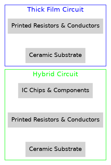
Thick film circuits and hybrid circuits are related but distinct concepts. A thick film circuit specifically refers to a passive circuit network formed on a substrate using thick-film technology – it includes printed resistors, capacitors, and interconnecting traces, emphasizing the fabrication technique itself. A hybrid circuit (also known as a hybrid integrated circuit), on the other hand, denotes a combined circuit on a single substrate that integrates multiple components, typically comprising a passive thick-film network plus attached active devices. In simple terms, a thick film circuit is often one part of a hybrid circuit, providing the passive functions and interconnections. In a hybrid IC, the ceramic substrate is first patterned with resistors, capacitors, and conductors via the thick film process, and then semiconductor chips (transistors, IC dies, etc.) are mounted onto it – together they form the complete circuit. Thus, the difference can be viewed as follows: thick film circuits focus on the process and materials, creating the passive components and wiring; hybrid circuits focus on the circuit integration level, combining a thick-film substrate with discrete semiconductor devices into one assembly. It’s worth noting that “hybrid circuits” can also be made with other techniques (like thin-film technology), but thick film is widely used in hybrids due to its relative simplicity and versatility. In summary, thick film technology provides hybrid circuits with a highly stable passive network and reliable interconnections, whereas the hybrid circuit as a whole results from incorporating active devices onto that thick film foundation to create a complete functional module.
3) Characteristics of Thick Film Circuits
Thick film circuits have a set of distinctive characteristics due to their materials and fabrication, giving them advantages in certain applications:
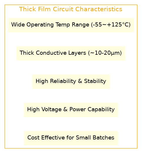
- Wide Operating Temperature Range: Thick-film ceramic circuits can function under extreme temperatures. Industrial and automotive-grade thick film circuits typically operate reliably from -55°C up to +125°C or more, with excellent stability through thermal cycles.
- Thick Conductive Layers for High Currents: Thick film conductors are on the order of tens of micrometers thick, much thicker than those in thin-film circuits. This allows thick film circuits to carry relatively higher currents and withstand high voltages.
- High Reliability and Stability: Thick film resistors are made of cermet (ceramic-metal) compounds (e.g. RuO₂-based glaze), which offer good long-term stability and low noise. The ceramic substrate is rigid and inert, unaffected by humidity or UV exposure.
- Flexible Design with Precision Tuning: By changing printed pattern geometries or using different paste compositions, the thick film process allows easy adjustment of resistor and capacitor values, enabling custom passive components. With laser trimming, device parameters can be precisely tuned to specifications (typical tolerance ±1%, or even 0.1%).
- Cost-Effective for Moderate Volumes: Thick film fabrication is relatively simple and well-suited for moderate volume, high-mix production. For medium quantities, it can lower unit costs by printing multiple circuits in one batch.
4) Typical Applications and Processing Details
Thanks to their stability and durability, thick film circuits are widely used in various electronic systems that demand high reliability. Typical application areas include aerospace electronics, communication and radar systems, industrial control circuits, as well as stringent automotive electronics modules. In such scenarios, thick film circuits often perform critical signal processing, precision sensing, or power control functions.
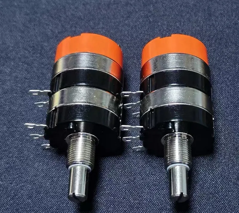
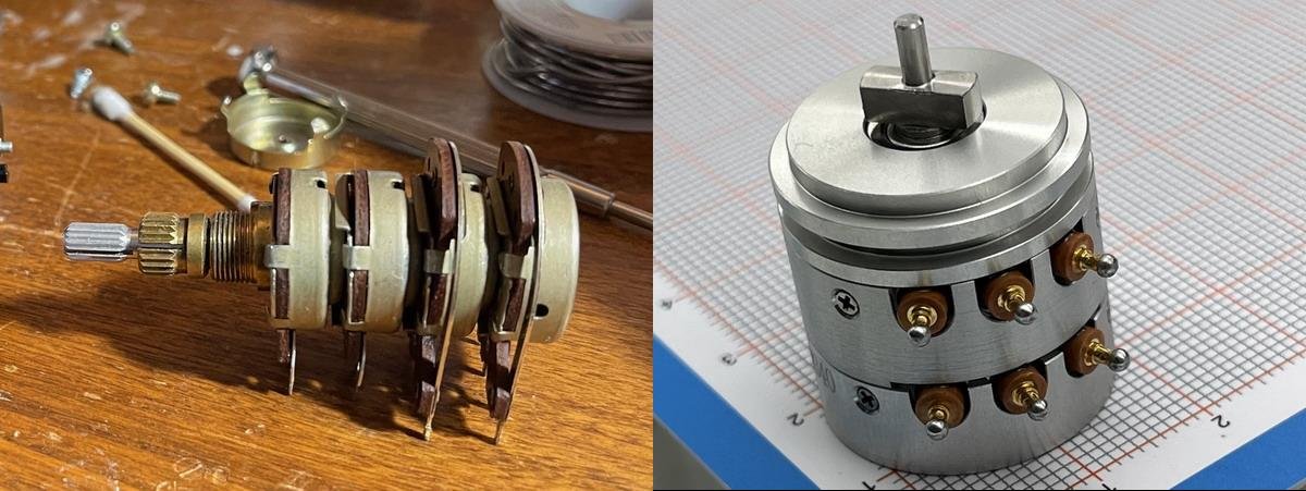
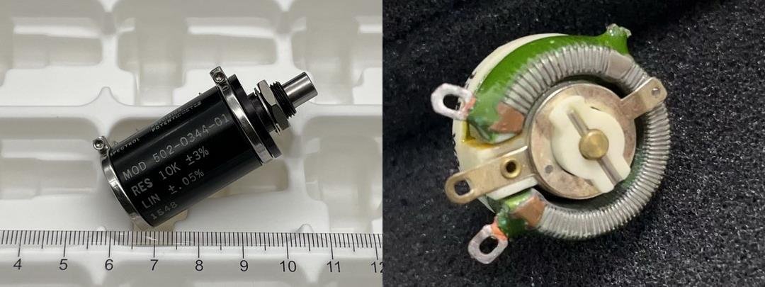
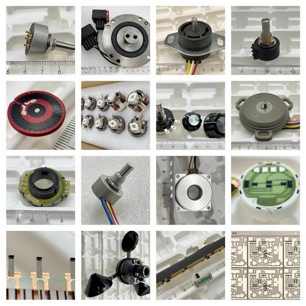
Beyond these high-end uses, thick film technology is also employed in manufacturing common electronic components like chip resistors and resistor networks. It is also used to produce heaters or potentiometers found in appliances and instrumentation.
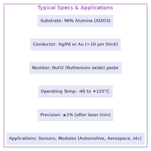
Standard thick film circuits use a 96% alumina ceramic substrate, typically 0.5–1.0 mm thick. Conductor material is often Ag/Pd alloy paste, forming metallic trace layers about 10 μm thick after firing. For high-reliability applications, Au paste is used. Resistor layers are made from ruthenium oxide-based pastes. Dielectric paste provides insulation for multi-layer builds. Typical line resolution is around 0.1 mm, and resistor tolerances can be adjusted to ±1% or even ±0.1%. The operating temperature range varies by application, such as -40°C to +125°C for automotive, and up to 150°C for aerospace.
5) Applications in the Automotive Industry
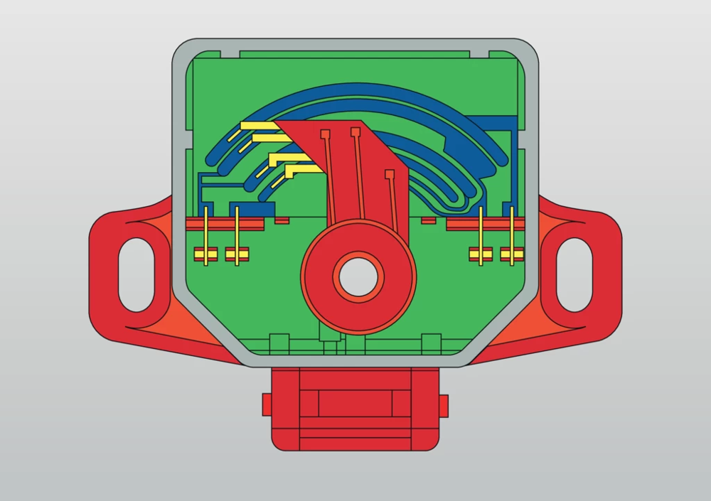
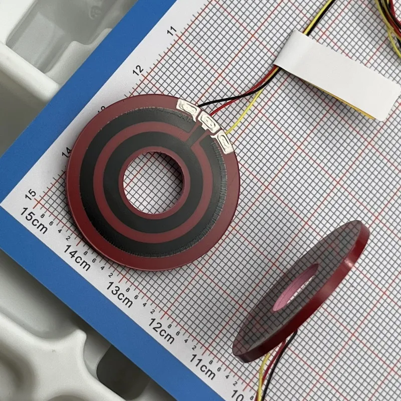
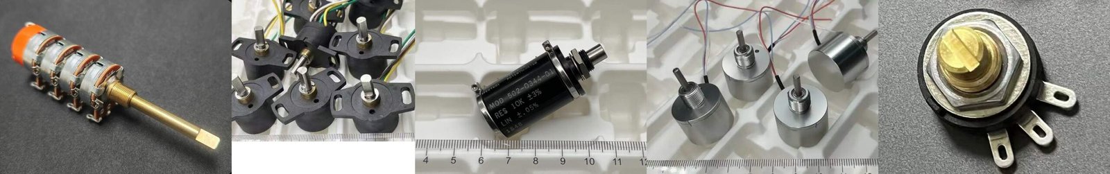
Automotive electronics demand high reliability and environmental tolerance, making thick film circuits essential in vehicle systems. Sensors and control modules use thick film circuits for robust performance. In angle sensors like throttle position sensors, a thick-film resistor and precious metal brushes form a variable resistor. As the throttle rotates, the brush slides over the resistive track, converting mechanical angle into voltage. This setup handles engine bay conditions like heat and vibration while maintaining output accuracy.
Other uses include pressure sensors with thick-film strain gauges on ceramic diaphragms, and fuel level sensors using float mechanisms with contact brushes over thick-film resistors. Thick film circuits ensure stable operation and smooth output.
Control modules like early ECUs, ABS controllers, and ignition modules use thick film hybrids for power control and signal processing. Ceramic substrates offer excellent heat dissipation and resilience in harsh environments. Despite trends toward high-density PCBs, thick film circuits remain vital in harsh automotive applications.
6) Relation and Significance of precious metal brushes
In thick-film potentiometric sensors, the precious metal brush is a key component. This precious-metal alloy wiper, mounted on a rotor, slides over the thick-film resistive track. The multi-finger brush ensures stable electrical contact, while the alloy offers excellent wear resistance and conductivity.
Such brushes extend sensor life to millions of cycles, maintaining signal stability in conditions like fuel vapor and high temperature. Multi-point contact ensures redundancy and minimizes signal dropouts. In environments like engine compartments, these brushes maintain low and stable contact resistance.
Together with thick film circuits, precious metal brushes enable long-lasting, reliable sensing. They are indispensable in automotive electronics and other variable-resistance sensing applications, supporting precise analog signal conversion.
7) Conclusion
Thick film PCBs bridge traditional PCBs and integrated circuits, offering high reliability and design flexibility. Their passive network capabilities support hybrid integrations, and their characteristics make them ideal for demanding applications. In automotive systems, they pair effectively with precious metal brushes to deliver precise and durable sensing solutions. With ongoing material and process advances, thick film technology will continue to play a vital role in sensor fusion, power modules, and harsh environment electronics.