Skip to content
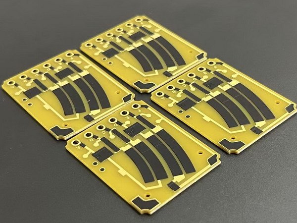
(The article is relatively long and is estimated to take 8–12 minutes to read.)
Thick film circuits combine durability with design flexibility, making them a key solution between traditional PCBs and integrated circuits. This article offers a comprehensive yet accessible dive into their principles, real-world use cases, design techniques, and future prospects.
Thick Film Circuits
Thick film circuits are a form of hybrid integrated circuit constructed by printing and firing layers of conductive, resistive, and dielectric materials onto a ceramic substrate. This technology enables passive components (like resistors) to be directly formed on the substrate, after which active devices such as semiconductor chips are attached, resulting in a compact and rugged electronic module. Serving as a solution between monolithic integrated circuits and traditional printed circuit boards, thick film circuits offer both high reliability and design flexibility. In this blog, we will explain the working principles of thick film circuitry, explore its practical applications, provide design guidelines for engineers, answer frequently asked questions, and look ahead to future trends of this technology.
Technical Principles
The fabrication of thick film circuits relies on screen printing and sintering processes. On a substrate (typically 96% alumina ceramic), conductive, resistive, or dielectric pastes are printed in circuit patterns layer by layer using precision screens. After printing, the substrate is fired at a high temperature (around 850°C is common), fusing the metal or metal-oxide particles in the paste into a solid film that adheres strongly to the ceramic surface. In contrast to thin film circuits (which require vacuum deposition of micron-thin layers and photolithographic patterning), thick film technology produces film layers on the order of a few to tens of micrometers thick — hence the name “thick” film.
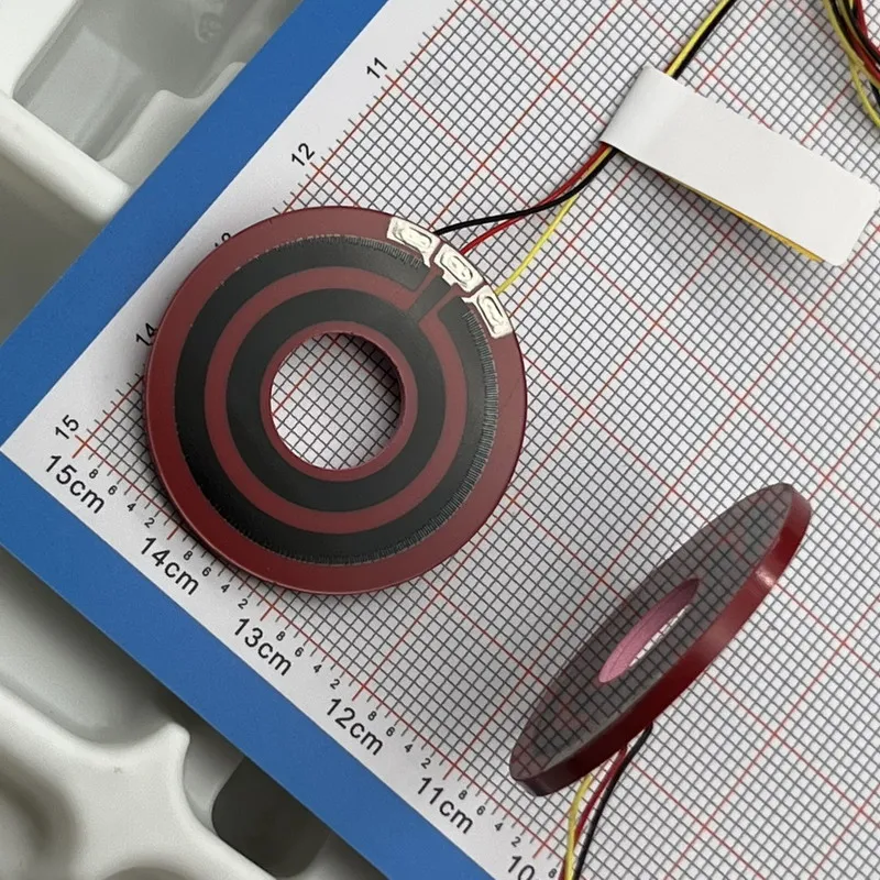
Complex interconnections in multi-layer thick film circuits are achieved by alternating printed conductor layers and insulating dielectric layers. The process begins with printing a base conductor pattern on the substrate, then printing a dielectric layer over it as insulation while leaving via holes where inter-layer connections are needed; subsequent conductor layers are then printed and fired, connecting through the vias as required. Through this sequential print-and-fire approach, thick film technology can build up circuits with multiple layers of wiring and cross-overs. For passive components, thick film resistors are formed by printing resistor paste in a specific geometric shape directly onto the circuit, and after firing, their values can be fine-tuned precisely by laser trimming (cutting away a small portion of the resistive film). Additionally, a small planar capacitor can be created by sandwiching a dielectric layer between two overlapping conductor areas. Once the circuit pattern is completed, discrete device chips (such as bare integrated circuit dies, transistors, etc.) are mounted onto the ceramic substrate and connected to the printed thick-film pads via gold wire bonding or soldering. Finally, the entire thick film hybrid circuit module is often encapsulated or hermetically sealed for protection.
The characteristics of thick film technology grant it unique advantages and some limitations in circuit design. On the one hand, the wide range of compatible materials allows engineers to choose different conductor inks (gold, silver/palladium blends, etc.) and resistor pastes to meet various requirements, enabling the integration of everything from milliohm-level heavy current traces to megaohm-level high-value resistors on the same substrate. Moreover, by adjusting a resistor’s printed geometry (length-to-width ratio) and selecting paste formulations, virtually any desired resistance value can be achieved, and combined with laser trimming, extremely tight tolerance matching is possible. On the other hand, compared to monolithic silicon integrated circuits, thick film technology can incorporate components that cannot be fabricated on a chip (for example, high-value capacitors, inductors, crystals — larger passive elements), and it allows multiple chips to be assembled together to realize a functional module. It should be noted, however, that feature sizes in thick film circuits are generally larger than those in thin-film or semiconductor ICs, and the initial tolerance and temperature stability of printed passive components (before trimming) are somewhat inferior to thin-film counterparts. Therefore, in practice, designers often must optimize the circuit layout and apply appropriate packaging or compensation techniques to balance performance with manufacturing considerations.
Practical Applications

Thanks to their ruggedness and reliability, thick film circuits found early and extensive use in aerospace and military electronics. Aircraft communication, radar, navigation, and guidance systems — as well as various electronic subsystems on satellites and spacecraft — have long employed thick film hybrid modules to withstand harsh conditions such as extreme temperatures, intense vibration, and cosmic radiation. In defense equipment, thick film circuits are commonly used as high-stability miniature functional modules, for example in precision sensor amplifier circuits, high-voltage power supply modules, and front-end signal conditioners. The automotive industry also adopted thick film technology early on for critical under-the-hood electronics. Applications included alternator voltage regulators, electronic ignition control modules, and early fuel injection driver circuits, and these thick film hybrids proved capable of enduring the heat and vibration of the engine environment with long-term reliability.
As the technology matured, the application range of thick film circuits expanded steadily into many civilian and industrial electronics domains. For example, in consumer electronics, thick film modules were once widely used in certain functional blocks of color televisions and audio equipment. In the 1970s and 1980s, you could find thick film hybrid modules inside TV sets handling tasks such as high-voltage regulation, switch-mode power supply control, video amplification, and audio processing — integrating complex analog circuits onto a tiny ceramic board for ease of assembly. In communications and computer hardware, thick film hybrids have been employed to create specialized function modules: for instance, RF/microwave components like voltage-controlled oscillators, band-pass filters, attenuators, and intermediate-frequency amplifiers in telecom base stations; as well as data converters, memory arrays, and regulator modules in early computer systems. In industrial control and instrumentation, thick film technology likewise plays a role — from multi-layer thick-film drivers for digital displays, to printed resistor strain gauges in sensors, and even miniature heating elements. Furthermore, in medical electronic devices, the drive for compact and highly reliable circuits has led to thick film hybrid circuits being used for analog front-end modules in equipment such as patient monitors and ultrasound systems.
Design Guidelines
Material Selection: Choosing the appropriate material system is the first step in thick film circuit design. The substrate is typically alumina ceramic (e.g. 96% Al₂O₃) for its excellent electrical insulation and thermal conductivity; if even higher heat dissipation or lower dielectric loss is needed, ceramics like aluminum nitride can be used. For special applications, thick film printing can even be done on substrates like stainless steel to meet unusual mechanical or environmental requirements. Conductor pastes are chosen based on the intended interconnect method: if wire bonding to chips is required later, a gold-based paste is used for printing the traces; whereas for attaching components via solder reflow, silver-palladium or silver-platinum alloy pastes are commonly used for the conductors. Resistor paste selection depends on the desired resistance range and temperature coefficient; manufacturers offer formulations spanning from a few ohms to hundreds of megaohms, so the appropriate paste can be chosen to provide the needed resistor characteristics in the design.
Circuit Layout: The circuit layout for a thick film design must take into account the resolution of screen printing and the properties of the materials. In standard thick film printing, the minimum achievable line width and spacing are on the order of 0.1–0.2 mm, so trace layouts should not be too fine or too tightly packed to ensure the paste can be printed continuously without breaks. If higher interconnect density is required, one can consider using photo-patternable thick film pastes, which allow line widths and gaps down to around 25 μm, suitable for high-frequency or high-density circuits. When routing conductors, sharp corners and abrupt width changes should be avoided to prevent electric field concentration and to ensure uniform paste deposition. Additionally, for circuits that must withstand high voltages, adequate creepage distances and clearances need to be incorporated into the design; if necessary, protective insulating layers or guard structures can be added to prevent dielectric breakdown. In multi-layer thick film designs, attention should also be paid to alignment tolerances between layers — via hole positions must be accurately aligned with the underlying and overlying conductor patterns to ensure reliable inter-layer connections.
Resistor Design & Trimming: Thick film resistors are implemented by printing resistor paste in a specific geometric pattern, with the final resistance value determined by the paste’s resistivity and the geometry of the printed shape. In the design, it is common to print the resistor such that its initial value is slightly lower than the target, and leave a small area at one end of the resistor (such as a narrow neck or a spiral section) for trimming. After the circuit is fabricated, laser trimming is used to cut away a tiny portion of the resistor film, thereby increasing its resistance to the precise target value. With accurate trimming, the tolerance of thick film resistors can be improved from an initial ±20% to within ±1% or better, meeting the needs of precision circuits. When precise matching of multiple resistors is required, it’s advisable to print those resistors in close proximity using the same paste batch, and trim them in the same session; this helps ensure they experience similar temperature drift and processing conditions, improving their relative consistency.
Component Integration & Interconnect: When integrating discrete devices on a thick film substrate, one must design appropriate mounting and interconnection structures for those components or bare chips. If using a bare die (unpackaged transistor or IC), the thick film layout should include metal pads of suitable size and shape to attach the die and to allow for gold wire bonding; the spacing and arrangement of these pads must match the chip’s bond pad layout, and the wire bond lengths should be kept as short and direct as possible to minimize parasitic inductance and ensure reliable connections. For designs using packaged components or surface-mount devices (SMDs), corresponding pads should be printed on the ceramic substrate aligned to the device leads, taking into account the requirements of solder reflow or conductive epoxy attachment — pad dimensions and spacing should meet the device’s footprint specifications. During the design phase, the final encapsulation or protection method should also be considered: if the circuit will be hermetically sealed in a casing, the height and placement of components must fit within the enclosure; if an organic potting or conformal coating will be applied, sensitive components should not be placed too close to package edges or feed-throughs. In short, component integration in thick film circuits requires careful coordination of electrical connections, mechanical mounting, and packaging protection to ensure the finished circuit is both electrically sound and physically robust.
Reliability Considerations: Thick film circuits, by virtue of their materials and construction, are inherently capable of high reliability, but certain design measures are needed to fully realize this potential. The thermal expansion coefficients of ceramic substrates and thick film materials are well-matched, meaning the layers expand and contract together during temperature cycling; however, for any interfaces where the thick film module connects to other substrates (like PCBs), differences in thermal expansion should be accounted for to avoid excessive stress. It is common to perform a burn-in process on thick film assemblies before final use to stabilize resistor values and other parameters. In the design, ensure thick film resistors and conductors have sufficient power and current margins — for instance, use wider traces for high-current paths and consider using multiple resistor elements in parallel or series to share power load if needed. For circuits operating in harsh conditions (humidity, salt spray, etc.), applying a protective overcoat on the circuit surface or using hermetic packaging is recommended to shield the thick film elements from environmental effects. In high-frequency applications, reliability also means long-term stability of performance, so the design should control stray capacitances and inductances to prevent circuit parameters from drifting over time. In summary, designing for reliability in thick film circuits involves addressing thermal, mechanical, environmental, and electrical factors to ensure the final product remains stable throughout its intended service life.
Frequently Asked Questions
Q: How do thick film circuits differ from thin film circuits?
A: The key differences lie in the fabrication process and the thickness of the deposited films. Thick film circuits use screen printing to deposit relatively thick patterns of paste onto a ceramic substrate, typically yielding film layers several microns or more in thickness which are then fired at high temperature; thin film circuits, on the other hand, are made by vacuum-depositing extremely thin layers of metals or dielectrics (usually less than 1 µm) and defining patterns via photolithography. Thick film technology can employ a wide range of materials (such as gold or silver-palladium pastes) to form multi-layer interconnects and directly incorporate passive components like resistors, and it tends to be cost-effective and convenient for small to medium batch custom circuits. Thin film circuits offer very high pattern precision and stable component parameters, but the process is more complex and typically limited to a single layer of interconnect; they excel in high-frequency and high-precision applications, albeit usually for relatively simple circuit structures.
Q: How does a thick film circuit differ from a conventional PCB?
A: The main differences between thick film circuits and printed circuit boards (PCBs) are in the materials and fabrication methods. A thick film circuit uses a ceramic substrate (like alumina) instead of the PCB’s organic fiberglass board, giving it much higher temperature resistance and thermal conductivity; its circuit traces are formed by printing and firing noble metal pastes, whereas a PCB’s traces are typically etched from copper cladding on a laminate. Thick film technology also allows passive components such as resistors or capacitors to be formed directly on the substrate, eliminating the need for mounting separate discrete parts as is required on a PCB. On the other hand, for large-scale planar interconnections, PCBs can be made larger and at lower cost, and multi-layer PCBs achieve complex routing by lamination of layers. In summary, thick film circuits are ideal for module-level circuits that require high reliability (e.g. high temperature or harsh environment tolerance) or the integration of special components, whereas PCBs are more common for general electronics with extensive wiring needs and mass production.
Q: How are precise resistor values achieved in thick film circuits?
A: Resistors in thick film circuits are first implemented by choosing an appropriate resistor paste and designing the printed resistor pattern to get close to the desired value, then fine-tuned to the exact value by laser trimming. During fabrication, the printed resistor is intentionally made slightly lower than the target resistance, and a portion of the resistor pattern is left available to be cut. After the circuit is produced and measured, a laser is used to cut a narrow groove (or grooves) in the resistor film, incrementally increasing its resistance until the desired value is reached. Using this laser trimming technique, thick film resistors can be calibrated to a very high precision, typically reducing error to on the order of one percent or less of the intended value.
Q: What about the reliability and lifespan of thick film circuits?
A: Thick film circuits, built on ceramic and fired thick-film materials, exhibit excellent reliability and long-term stability. With proper design and packaging, they can operate for extended periods in harsh conditions. The ceramic substrate is non-hygroscopic, and the noble metal conductors plus metal-oxide resistor films are chemically stable after firing, so thick film circuits are highly resistant to temperature cycling, mechanical shock, and vibration. Many thick film modules in aerospace and automotive systems have been in service for decades with sound performance. It’s worth noting that thick film resistors may have a slight initial drift, which is why a burn-in process is often used to stabilize them before final use. Also, thick film circuits should be protected from excessive moisture or corrosive environments, typically by an encapsulant or seal, to prevent any long-term degradation. With proper protection and operation within rated limits, the lifespan of a thick film circuit can be as long as the lifetime of the components it contains.
Q: Are thick film circuits suitable for mass production?
A: Thick film circuits can be produced in small custom batches or at a moderate volume, but their cost-effectiveness relative to PCBs or ICs depends on the application. For medium-volume production of specialized modules (for example, thick film sensor circuits in automobiles or thick film resistor networks), the thick film process can achieve batch fabrication by printing many circuits on a single large ceramic panel, firing them together, and then dicing the panel into individual units, which improves throughput. The upfront tooling for thick film (screen masks) is relatively inexpensive, and changing a design incurs minimal cost, which is advantageous for small-to-medium volume manufacturing. However, for very high-volume products with extensive circuitry (such as large boards in consumer electronics), traditional PCBs tend to have a cost advantage on a per-unit basis, as PCBs can be manufactured on high-speed automated production lines at low material cost. In summary, thick film circuits are well-suited to products that demand special performance and reliability — they can indeed be mass-produced to a certain extent by optimizing the process — but for purely cost-driven high-volume electronics with large layouts, PCBs remain the primary choice for interconnection.
Future Trends
As a well-established electronic fabrication technique, thick film circuitry continues to evolve to meet the needs of emerging applications and higher performance demands. One clear trend is toward finer feature sizes and higher frequencies: by introducing photo-patternable thick film pastes and improved printing methods, the achievable line widths and spacings in thick film circuits are shrinking, which broadens their use in RF and microwave domains. Today, thick film processes can achieve features on the order of 25 μm or even smaller, meaning thick film microwave circuits can operate at tens of gigahertz, supporting high-frequency applications like 5G communications and automotive radar. At the same time, multi-layer ceramic substrate technologies (such as LTCC – Low Temperature Co-fired Ceramic) combined with thick film printing are enabling three-dimensional interconnect structures and high integration modules, positioning thick film technology as a key player in high-density packaging and modular devices. New developments in materials are also noteworthy, such as the adoption of lead-free thick film pastes, the development of resistor compositions with improved stability, and polymer-based thick film processes that can be printed on flexible substrates — all of which open up new application possibilities for thick film technology.
Moreover, changing application demands are steering thick film circuits in new directions. In the automotive electronics sector, with the rise of electric vehicles and autonomous driving, there is a growing need for sensors, power modules, and high-temperature high-reliability electronics in vehicles. Thanks to its ability to withstand high temperatures and integrate complex functions, thick film technology is poised to play a continued role in EV power control units, battery management systems, and various environmental sensors. In the industrial IoT and sensing arena, thick film processes can be used to manufacture all kinds of printed sensors (for example, the sensing films of gas sensors or the Wheatstone bridge networks of pressure sensors), meeting requirements for miniaturization and cost-effective volume production. It is worth noting that many discrete passive components (such as chip resistors and heater elements) are themselves made using thick film techniques — a testament to how deeply thick film processes have penetrated