Skip to content
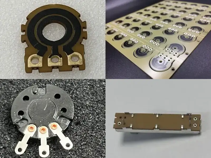
Why I Wrote This Post
Recently, I discussed a custom potentiometer assembly with a German customer. The customer had special needs for budget, performance, and secondary processing. My colleagues and I reviewed common substrates used in potentiometers. It was interesting, so I wrote it down for reference.
The customer first wanted a new resistive element and new tooling. But the pin shape requirement was strict. The customer also wanted to solder the pins by themselves. After overall evaluation, we recommended an existing product with the same appearance, but with upgraded materials and processes. This helps avoid new tooling cost. Tooling includes screen-print layout and substrate forming molds.
For assembly or kit buyers, the real question is not “which material is more premium”, but what will actually work in production and in use, such as:
- Which material and process can meet the usage requirement?
- Will there be issues during processing or secondary processing?
- During custom replacement, can the new process keep the full function of the original product?
- Why can similar carbon track assemblies have big differences in price and reliability?
In this post, I will use 5 typical photos as a guide. Then I will share four tables: application table, performance table, process route table. If you are an application buyer, this can help you explain needs faster and choose a route that can be produced in volume.
Part 1 | Photo Guide: Understand Differences with 5 Samples
Five photos: fiberboard, customer phenolic plate, bakelite, FR4, and glass fiber with copper pads.
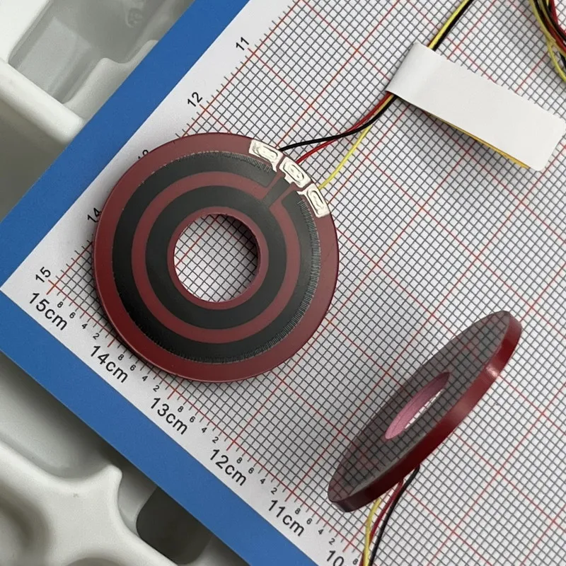
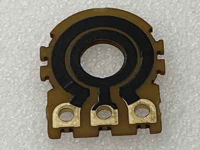
Fiberboard + Silver Paste Connection (Our Sample)
- Substrate + conductor system: phenolic-based plate (paper-based or fabric-based reinforcement is common) + silver paste conductor (the customer sample uses air-dry silver paste).
- Connection method: high-temperature soldering is usually not recommended. Low-temperature methods are more common, such as press-fit, riveting, or conductive adhesive.
- Key point: carbon printing often needs baking/curing. So we prefer a baked system for carbon and metal tracks. But this type usually cannot accept a 260 to 280°C solder peak. The silver layer at the connection area may be damaged and cause performance problems.
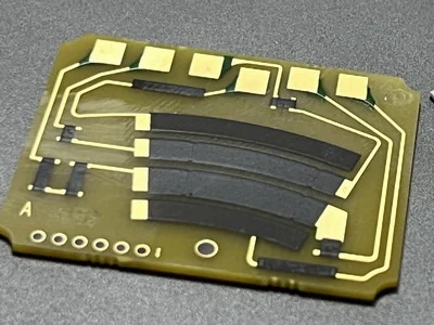
Customer Phenolic Plate Dual-Track Assembly: Carbon Track + Silver Track
- Substrate + conductor system: linear assembly with dual tracks. One carbon track plus a printed and cured silver layer.
- Connection method: depends on terminal-area metallization or copper pads, and the assembly requirement.
- Key point: dual tracks are usually not for show. They split different functions into different tracks, so the output can be more stable.
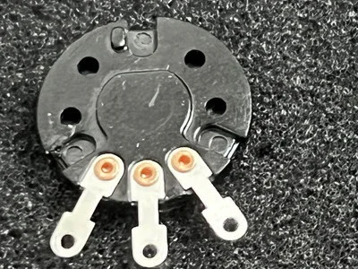
Round Potentiometer and TPS (Copper-Clad FR4) Solderable Option
- Substrate + conductor system: copper-clad FR4. It is basically a PCB pad system.
- Connection method: the terminal area can be soldered. This is one of the most universal assembly routes.
- Key point: the carbon track is usually printed on an insulation layer. Copper is not kept under the track. Copper pads stay at the terminal area for soldering.
Round Bakelite
- Substrate + conductor system: bakelite is also part of the phenolic family.
- Connection method: the terminal-area design decides the final connection process. Multi-track designs are more sensitive to boundary and overlap control.
- Key point: hardness is higher than fiberboard and lower than ceramic. Forming is easier.
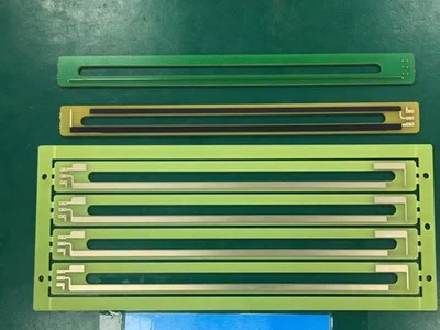
Glass Fiber Substrate + Local Copper at Terminal Area (Copper Pad Solder Points)
- Substrate + conductor system: glass fiber plate. Copper is only at the terminal area. The solder points are confirmed as copper pads.
- Connection method: the terminal area is solderable. Other areas follow the track design and insulation needs.
- Key point: do not judge solderability by color. Confirm if the terminal area is a copper pad system, and if copper coverage reaches the hole and pad edge.
Part 2 | Customer Case Analysis: Also Explaining the Structure of Carbon Film on PCB
1) The Sample Provided by the Customer and the Resistive Element Structure They Wanted (Cross-Section View)
This also explains why I felt this customer had a very clear and serious idea of what they wanted.
He had a fairly clear understanding of the whole resistive element structure. He had even already considered whether the joint area needed silver paste, or whether extra solder points should be added for reinforcement.
He even specifically asked me to confirm whether this step was necessary.
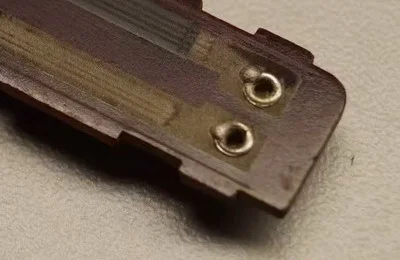
Please see the figure below. The drawing was made by the customer, and the cylindrical pins can also be seen in it.
2) We First Analyze the Features of the Customer’s Sample, and at the Same Time Go Through the Substrate Selection Logic and Answer a Few Related Questions
Because this part is still mainly based on visual analysis, I will first explain the logic behind my judgment. The final conclusion should still be based on actual sample testing.
-
In the customer’s dual-track structure, one track is carbon film, and the other track is a silver layer.
This is actually quite similar to the common structure used in audio faders.
At the same time, the customer also mentioned logarithmic output, so based on this information together, I believe it is more likely used in audio equipment with relatively higher requirements. -
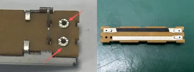
The four pin holes use a hollow stamping and flanged riveting process, and then self-drying silver paste is applied. One purpose is to improve conductivity, and the other is to further reinforce the solder joint area.
- As can be seen from the figure above, the holes were made by hollow stamping, but no embossing was added afterward.
From this detail, it seems that the selected substrate at that time, which was phenolic board, was still somewhat weaker in strength and toughness, so embossing reinforcement was not added afterward.
Of course, whether embossing is used in real production may also be affected by cost, process habits, production volume, and other factors. It may not be caused by the material alone.
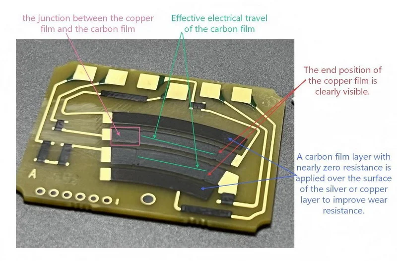
Now let us look at the hole area of a commonly used fiber board in the figure below. It uses embossing to improve fastening strength, and both front and back side images are shown.
- Here I also found a TPS sample where the carbon film joint area can be seen more clearly, and it can be used to answer the customer’s earlier question.
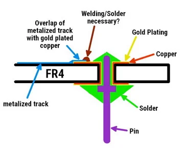
If FR4 is used as the substrate, then reinforcement such as welding / solder is usually no longer necessary in this area.
At the same time, this image can also show the thick-film structure on a normal PCB board more clearly.
3) At This Point, the Substrate Selection Logic in This Case Is Already Basically Clear
On the surface, this may look like only a secondary process choice.
But in fact, it is essentially also a choice between a high-temperature process and a low-temperature process, and it directly affects how the substrate should be selected.
It can also be understood as a situation where there is also a cost conflict in substrate selection.
In this case, fiber board is no longer a very suitable choice.
This is because the melting point of the low-temperature silver layer is about 220°C, while the more reliable temperature for solder connection is usually around 260°C to 280°C.
As a result, the low-temperature silver layer can be easily damaged by the higher temperature during soldering.
So at this point, we are more inclined to choose FR4, which can also be directly understood as using a PCB board as the substrate.
In the end, the finished product will follow the same outline logic as the earlier fiber board version, but the material will be changed to FR4.
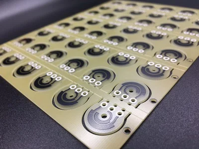
Its appearance would be like the figure below:
Part 3 | Application Comparison Table
When customers name a material, they often mean a connection method and process window. This table helps application buyers find the closest route.
| Substrate (Common Name) | Typical Use (Application View) | Reason (One Line) | Terminal Connection (Common) | Notes (Confirm First) |
|---|---|---|---|---|
| Phenolic-based plates | Low-cost insulation base, printed conductor or resistor parts with low-temp connection | Cost sensitive, easy processing | Press-fit, riveting, conductive adhesive | “Phenolic” is a broad term. Paper-based vs fabric-based reinforcement changes strength. Silver paste also varies (air-dry vs baked). Low pressure strength. Easy to crack. |
| Bakelite (a phenolic term) | Insulation structural parts, assemblies needing higher rigidity and insulation | Good insulation, high hardness, easy structure | Insert terminals, riveting, press-fit (solder depends on metallization) | Can be molded parts or machined sheets. It depends on structure and cost target. |
| Fiberboard | Linear pot or sensor base | About 200 gf hardness with toughness, better terminal-hole impact strength | Terminal fixing, riveting, press-fit, or local metallization | Better for larger fixing actions. Terminal hole area is more stable. |
| Copper-clad FR4 (PCB) | Assemblies needing solder pads and routing | Mature process, universal for assembly | Soldering (copper pads at terminals) | Carbon track is usually printed on insulation. Copper pads remain at terminals. Cost is relatively higher. |
| Glass fiber with local copper pads | Need stability and solderable terminal area | Strong connection compatibility | Soldering (copper pads at terminals) | Copper only at terminal area. Confirm copper coverage and hole structure. Cost is relatively higher. |
Part 4 | Performance Comparison Table
This is not a full material encyclopedia. It lists the key factors affecting carbon tracks, metal layers, and terminal reliability. Without consistent tests, avoid absolute insulation numbers. Relative wording is safer.
| Substrate | Hardness (gf, your reference) | Key Mechanical Point (Common Risk) | Thermal Process Window | Solderable at Terminal Area (Strict Wording) | One-Line Tip |
|---|---|---|---|---|---|
| Phenolic-based plates | (not fixed) | Strength and impact resistance vary a lot by paper-based vs fabric-based | Low to medium (mostly decided by conductor system) | Depends on copper or metallized pads. Silver paste joints should not take solder peak | Mostly phased out in mid to high-end fields |
| Bakelite | ≥200 (your current reference) | Harder than ABS, lower than ceramic. Good insulation. Easy forming | Medium to wide | Depends on metallization or insert terminal structure | High voltage insulation. Good for high insulation needs |
| Fiberboard | ~200 | Terminal holes take more impact. Fixing action can be more stable | Medium to wide | Depends on metallization or copper pads | Cost-effective and widely used |
| Copper-clad FR4 | (N/A) | Highly standardized process | Wide | Yes (copper pad system at terminals) | Used in mid to high-end. Solderable |
| Glass fiber with local copper pads | (N/A) | Good stability. Copper pads at terminals | Wide | Yes (copper pads at terminals) | Similar to FR4. No need to copper-clad under the silver layer |
Part 5 | Process Route Comparison Table
For similar carbon assemblies, cost differences often come from the process route: metal layer method, carbon curing, terminal transition into a reliable joint, and boundary control. Clear constraints make selection faster.
| Substrate | Carbon Track Method | Metal Conductor Method | Final Terminal Connection | Key Risk (Reminder) | Cost Driver |
|---|---|---|---|---|---|
| Phenolic-based plates | Printed carbon, needs baking/curing | Air-dry or baked silver paste. We prefer baked system for carbon and metal tracks | Press-fit, riveting, conductive adhesive (unless terminal is metallized) | Avoid 260 to 280°C solder peak. Heat can damage the silver joint | Yield and rework, adhesion, boundary control, curing profile, assembly structure |
| Bakelite | Depends on structure and targets | Depends on structure and targets | Insert terminals, riveting, press-fit | Long-term stability depends on terminal structure and stress transfer | Molding vs machining changes cost |
| Fiberboard | Printed carbon (often baked) | Silver paste or metal track depends on the project | Terminal fixing, riveting, press-fit, or metallized terminal area | Impact and stress during fixing. Looseness can cause instability | Low cost |
| Copper-clad FR4 (PCB) | Carbon printed on insulation layer. No copper under track | Copper pad system at terminals | Soldering | Heat influence near boundaries | PCB process and pad design, higher cost |
| Glass fiber with local copper pads | Carbon printed on insulation area (optional overcoat) | Copper pads only at terminal area | Soldering at terminal area | Confirm copper coverage and hole structure. Avoid heat affecting sensitive areas | More complex pad design, higher cost, better compatibility |
Part 6 | General Selection Guide (Quick Table)
This table is based on common constraints from application buyers. If you clarify assembly method, temperature limits, and cost target, you can quickly lock a workable route.
| Typical Requirement | Recommended Route | Common Substrates | Keywords | One Question to Confirm |
|---|---|---|---|---|
| Need secondary soldering later | Choose terminal copper pads first | Copper-clad FR4, glass fiber with local copper pads | Solderable, pads, copper, plated hole | “Are the solder points copper pads? Is copper full coverage or only at terminal area?” |
| Cost control is the main goal | Silver paste system + low-temp connection | Phenolic plates, fiberboard (depends on assembly impact) | Silver paste, press-fit, riveting, conductive adhesive | “Is the fixing action heavy? Any vibration? How are terminals fixed?” |
| Terminal holes must take heavy fixing action | Focus on terminal-hole impact resistance | Fiberboard | Terminal hole, riveting, impact | “Riveted or press-fit terminals? How strong is the fixing action?” |
| Need high voltage insulation | Insulation structure first | Bakelite or phenolic system, sometimes glass fiber | Clearance, creepage, insulation | “Max working voltage or surge voltage? Any clearance or creepage requirement?” |
| Big temperature and humidity changes | Stability and moisture resistance first | FR4 or glass fiber system | Moisture, drift, long-term | “Temperature and humidity range? Any condensation or salt fog?” |
| Very stable output, low noise or jitter | Multi-track gives more room (higher cost) | Choose by connection method | Dual track, 4 track, boundary overlap | “Is the target noise, linearity, or contact stability? What is the cost limit?” |
| Tight lead time | Choose mature process route | FR4 or glass fiber pads, or mature phenolic + silver | Mature process, yield | “What alternatives are acceptable? Which parameters must not change?” |
Final Notes
I wrote this article to explain one key point that is often missed: the substrate sets the process window, the process window sets the connection method, and the connection method often decides stability and rework cost.
If you only have photos or samples and no full drawings, it is still fine. If you can clearly show the terminal area (holes and pads) and the track area (carbon and metal), we can first decide the main route—solderable or low-temperature connection—then cost and lead time become much easier to discuss.